


-
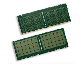
A substrate for the ever quickly increasing flip chip connection method by miniaturization and thinning the said electronic equipment. Contributing to the miniaturization of the implementation area.
*Flip Chip Connection Method ... Electrically connecting between the substrate and LSI chip through an ultra fine "metallic protruding electrode" called "bump." The connection between the bumps that are bridged electrically between the substrate and LSI chip is done by changing the bump shape with an application of pressure at high temperatures, or by adhering among the metals using heat fusion.
-
Features
- Our company has responded to the demand of multiple pins (pitch narrowing and secure bat width) for high integration and multiple functionalities by creating an ultra fine wiring production technology.
-
Applications and Final Products
- Suitable mainly for small electronic equipment and portable equipment such as cellular phones, laptops, small calculators and digital cameras.

-
Main Specifications
Layers Hole Diameter L/S Board Thickness 2 Layers, 4 Layers 100μmΦ 30/30 120μm~400μm -
Product Inquiries
- Domestic Sales Division
- Tel : 0266-71-1562
- Fax : 0266-73-3366